MidFlorida Materials & Characterization offers more than 40 years direct experience in the analysis and characterization of materials using a wide range of X-ray methods. Below is a subset of some of the analyses that we have performed in the past. We would welcome the opportunity to share our knowledge with you in order to help solve your materials analytical problems!
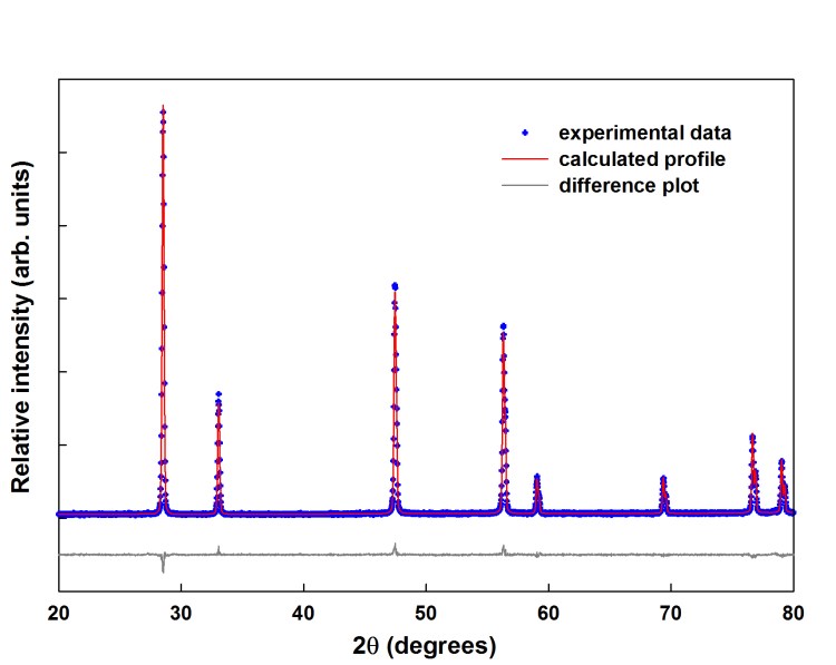
- Powder X-ray diffraction: Deep experience in both qualitative and quantitative methods for powder X-ray diffraction for materials characterization, including phase identification using PXRD databases. The diffraction scan from NIST SRM674b (CeO2) shows a typical high quality PXRD scan
- Thin film XRD: Optimization of X-ray diffraction methods for polycrystalline thin film analyses. On the right is a diffraction scan recorded from a sample consisting of 90nm Cu with a 20nm Pt layer; note the both as-deposited layers are clearly distinguished
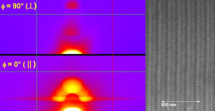
- Grazing Incidence small-angle X-ray scattering (GI-SAXS): GI-SAXS permits the measurement of nanostructured materials without the need or regard for crystallinity. The Figure shows two GI-SAXS patterns recorded at different azimuthal settings from a 50nm sSu grating. The difference in scattering is attributed to the grating sidewalls; note that these data were obtained with a laboratory system.

- Critical dimension small-angle X-ray scattering (CD-SAXS): Like GI-SAXS, CD-SAXS is insensitive to the details of crystal structure in nanostructured systems. It is rapidly evolving into a primary tool for metrology of ultra-small transistor structures in advanced semiconductor device manufacturing. The Figure shows a data construct from a synchrotron CD-SAXS analysis of FinFET devices that showed key details of the nanoscale device structure
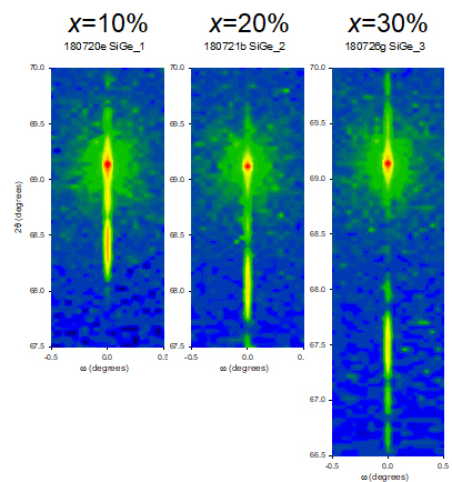
- High resolution triple axis XRD: For many years we have used high-resolution double- and triple-crystal XRD methods to study the properties of defects in otherwise highly perfect single crystal materials. The measurement of strain and structural defects is of course a subject of major interest to the semicon-ductor industry. The use of advanced approaches such as high-resolution triple-axis reciprocal space maps (RSMs) such as those shown here from Si-Ge heterostructures are important for showing the effect of materials processing on semiconductor properties.
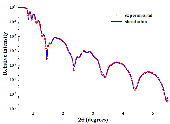
- High resolution triple axis XRD: X-ray reflectometry (XRR): Like the SAXS methods described above, low-angle specular XRR is not sensitive to the crystalline structure (or lack of crystallinity) in a thin film structure. At Mid-Florida Materials & Characterization we have deep experience in all aspects (hardware, software, experimental details, and benefits/pitfalls) of XRR characterization of thin film materials, such as the Cu/Ta/Si film stack used for the figure on the right.
Other X-ray analytical methods: At MidFlorida Materials & Characterization we have both an understanding of the breadth of X-ray tools for materials charac-terization as well as hands-on experience in using most of them. For diverse approaches involving texture or preferred orientation, residual stress, single crystal orientation, or whatever — if it involves X-rays, we can help you!
